
By Assaf Carlsbad & Itai Liba
Hello and welcome back to the 4th part of our blog posts series covering various aspects of UEFI internals and exploitation. In the last three posts, we mostly covered the necessary background information to help us bootstrap our journey into UEFI land. We culminated by developing our own coverage-guided fuzzer on top of the Qiling emulation framework and AFL++ that can be used to fuzz the contents of NVRAM variables.
During the course of these three blog posts, our interaction with UEFI code was mostly mediated through software emulation (backed by the amazing Qiling engine). While very accessible and cost-effective, this blog post will explore firmware code via a slightly different approach. As such, most of our interactions will be with a live, physical system. The main motivation for this paradigm shift came from a somewhat innocent attempt to run a CHIPSEC module which goes by the name common.uefi.s3bootscript:
The common.uefi.s3bootscript module is in charge of locating, parsing and validating a piece of memory commonly referred to as the “S3 boot script”. In a nutshell, the S3 boot script is a data structure that lists the actions the firmware must take in order to correctly recover from the S3 sleep state. Unfortunately, at least on our own testing machine, (Lenovo ThinkPad T490) this CHIPSEC module consistently failed with a somewhat cryptic error message: “S3 Boot-Script was not found. Firmware may be using other ways to store/locate it”.
For the average security researcher, such phrasing immediately raises a series of follow-up questions, such as:
- How exactly does CHIPSEC try to locate the boot script?
- What are the “other ways” the firmware might be using to store it?
- Can we find some alternative methods to extract and parse the boot script?
Like most other things in life, the motivation for answering these questions is threefold:
- Visibility: Normally, we tend to think of the firmware as an obscure, big blackbox that provides very limited visibility to what is actually happening under the hood. Knowing exactly what the firmware is doing to recover from S3 sleep state can definitely shed some light on the subject and help us reveal the underlying implementation of some low-level components and interfaces.
- Vulnerability hunting: Historically, naive or just plain bad implementations of the S3 boot script were subject to a myriad of attacks. Because the system is not yet fully configured by the time the boot script executes, hijacking control flow at this point in time allows attackers to disable or completely bypass certain security features offered by the platform. By knowing how to locate, extract and parse the boot script we can validate its integrity and assess its resilience against these kinds of attacks.
- Fun: Last but not least, this can be a very interesting challenge on its own which also puts into test a lot of the knowledge that we gathered around UEFI in particular and firmware security in general.
The S3 Boot Script
Before moving on to explore some actual techniques for dumping the boot script, it’s important to take some time to understand the rationale behind it. The S3 sleep state was introduced by the ACPI standard for power management, alongside some additional low-power states labeled S1, S2 and S4. Lets go over them briefly:
- S1 is the Standby state. This is a low-wake latency state, where no CPU or chipset context is lost.
- S2 is currently not supported by ACPI.
- S3 is the suspend-to-RAM state. It is similar to the S1 sleep state except that the CPU is turned off and some chips on the motherboard might be off as well. Power to main system memory, on the other hand, is retained. After the wake event, control starts from the processor’s reset vector.
- S4 is the suspend-to-Disk state (hibernation). It is the lowest power, longest wake latency sleeping state supported by ACPI. It is usually implemented by writing an image of memory into a hibernation file before powering down. Upon resumption, the system restores its context from the saved hibernation file on disk.
As has already been mentioned, UEFI breaks the boot process into multiple distinct phases, each with its own responsibilities and limitations. During a normal boot, the PEI phase is responsible for initializing just enough of the platform’s resources to enable the execution of the DXE phase, which is where the majority of platform configuration is performed by different DXE drivers.
However, to speed up booting from S3 sleep UEFI provides a mechanism called a “boot script” that lets the S3 resume path avoid the DXE, BDS and TSL phases altogether. The boot script is created during normal boot with the intention of being consumed by the S3 resume path:
- During a normal boot, DXE drivers record the platform’s configuration in the boot script, which is saved in NVS. The boot script is comprised out of a series of high-level “opcodes” which are to be interpreted by a boot script execution engine. These “opcodes” include reading from and writing to I/O ports, PCI devices, main memory, etc. For the complete list of supported opcodes, please refer to PiS3BootScript.h.
- Upon resuming from S3 a boot script engine executes the script, thereby restoring device configurations that were lost during sleep. Schematically, the relationship between the PEI phase, DXE phase and the S3 boot script can be depicted as follows:
For a more thorough discussion of the S3 boot script and its role in restoring the platform’s configuration, please refer to this document.
Digging Deeper
Now that we know what the S3 boot script is all about, let’s try to get a clearer picture of what went wrong with CHIPSEC.
To do so, we’ll run a command to dump it again, this time with the --hal and -v command-line switches for augmented verbosity:
From the output of the command we can clearly see that in order to get the contents of the boot script, CHIPSEC first tries to search for an EFI variable named AcpiGlobalVariable.
The exact definition of the structure that backs up this variable can be found in AcpiVariableCompatibility.h taken from the ModernFW repository:
Taking padding into account, offset 0x18 of the structure contains the AcpiBootScriptTable member which holds the physical address of the boot script in memory. Now that we know for sure the pointer to the boot script is encapsulated inside AcpiGlobalVariable, let’s try to figure out why CHIPSEC failed to find it. To do so, we’ll run the chipec_util uefi var-find command that lets us query and probe for the presence of EFI variables:
Unfortunately, it seems that for some reason CHIPSEC failed to find or query this variable altogether. After digging through some old EDK2 commits, we eventually managed to pinpoint the reason for this in a commit dating back to 2014 that removed the runtime attribute from AcpiGlobalVariable. As was mentioned in the previous blog posts, variables that don’t have the EFI_VARIABLE_RUNTIME_ACCESS attribute cannot be queried from the operating system and are only accessible for the duration of the boot process (i.e., before the boot loader calls ExitBootServices).
Now that we understand the root cause of the problem, the question is whether we can come up with some clever tricks to extract the boot script in spite of the fact that the variable that contains it is inaccessible to us. It turns out that not only is the answer to this question positive but also that we have at least two distinct ways at our disposal to do so.
Method #1: Reading AcpiGlobalVariable From an Offline Dump
By now we know that AcpiGlobalVariable doesn’t have the EFI_VARIABLE_RUNTIME_ACCESS attribute, and therefore it can’t be enumerated from the OS. Alas, these restrictions only apply to a live, running system. In other words, as long as this variable exists physically on the SPI flash there is nothing to prevent us from reading it using an offline dump of the firmware.
Given that premise, we can devise the following “algorithm” for reading the S3 boot script:
- Dump the UEFI firmware to a file (can be done simply by running
python chipsec_util.py spi dump rom.bin, and see part 1 for more details).
- Open
rom.binin UEFITool and search forAcpiGlobalVariable. Use the ‘Body hex view’ option to read the contents of this variable and interpret the data as a little-endian pointer. This pointer should hold the physical address of theACPI_VARIABLE_SET_COMPATIBILITYstructure in memory.
- Feed this address into a physical memory viewer such as RW-Everything, and read the QWORD value at offset 0x18 (corresponding to the
AcpiBootScriptTablemember)
- Now, cross your fingers and pass this address as an additional argument (
-a) to CHIPSEC. If all goes well, CHIPSEC should now be able to parse the boot script and scan it for any potential vulnerabilities.
After we uncovered the boot script in physical memory this way, we tried modifying it for the sake of disabling certain security measures. However, after completing a full sleep-resume cycle, the contents of the script were “magically” restored. This strongly suggested that the pointer we obtained only points to a copy of the boot script, while the source is saved someplace else. Cr4sh probably encountered this phenomenon back in 2016, which is why he writes:
Now, all we have to do is understand what an SMM LockBox is and how we can extract the boot script out of it.
Method #2: Extracting the Boot Script From an SMM LockBox
As mentioned earlier, the S3 boot script is in charge of restoring the platform’s configuration to its pre-sleep state. This usually includes re-enabling and locking various security settings which were lost during sleep. Because of its sensitive and privileged nature, the boot script itself must be kept in a memory region which is guarded against malicious attempts to modify it. The main problem is that the threat vector includes not only attackers with user-mode permissions but also local attackers with kernel-mode privileges. Given that kernel-level code has full access to physical memory, how can the firmware store the boot script such that it will be tamper proof?
A Whirlwind Tour of SMM
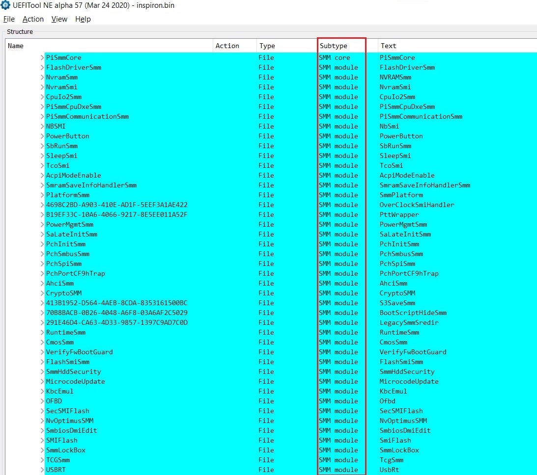
Enter SMM. SMM, or System Management Mode, is one of the operating modes found in every Intel-compatible CPU and dates back to the old i386 days. Historically, SMM was intended to provide firmware developers with an isolated execution space where they can implement support for features such as APM (Advanced Power Management), Plug-and-Play and so on. Over the years, OEMs started shifting more and more of their proprietary code base into SMM, and the end result is that a typical firmware image usually contains a magnitude of dozens of different modules that all operate in this mode.
Schematically, the relationship between SMM and the other, more familiar operating modes of the CPU is usually depicted in the Intel manuals as follows:
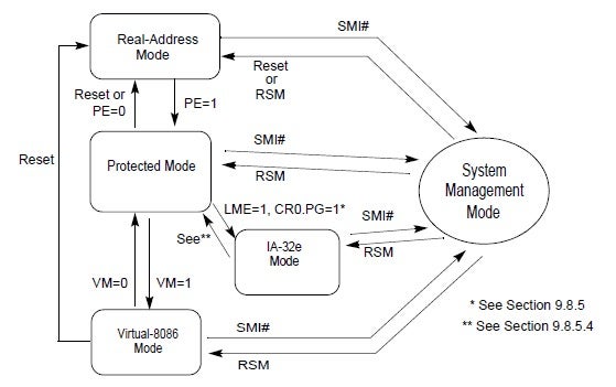
From the figure above, some important facts about SMM can be deduced:
- The processor transitions from its current operation mode to SMM in response to a System Management Interrupt, or SMI for short. The exact nature of these SMIs will be discussed in the next section.
- Transition to SMM can happen from every CPU mode and is completely transparent to the operating system. That means that when an SMI is triggered, the operating system’s kernel is preempted and control is passed to a dedicated routine called the
SMI handler. - After the SMI handler finishes servicing the interrupt, it can make the processor exit SMM and return to its previous state by executing the rsm instruction.
System Management Interrupts
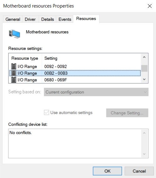
A typical computer contains a plethora of different devices that are capable of generating an SMI. Still, from the perspective of any security-oriented research, the most important SMI source is the software-generated SMI. This type of SMI can be triggered synchronously by software, given it is running with ring 0 (kernel) privileges. To generate a software SMI, we take advantage of the APM chip found on virtually every Intel-compatible computer.
The software interface to the APMC consists of two I/O ports: 0xB2 and 0xB3.
- Port 0xB3 is usually referred to as a status port, even though this description might be a bit misleading. In practice, it is used as a scratchpad register that can be written freely by software.
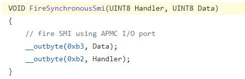
- Port 0xB2, on the other hand, is the code port. Writing a single byte to this port using the outb instruction causes the APM chip to assert the SMI# pin of the processor.
A common pattern to generate a software SMI using these two I/O ports is as follows: first, pass any arguments to the SMI handler by writing them to port 0xB3. Afterwards, write port 0xB2 to actually trigger an SMI. In case the firmware offers several different SMI handlers, the exact byte value written to port 0xB2 can be used to select the particular handler to invoke. This idea is demonstrated clearly in the ThinkPwn exploit by Cr4sh:
Communicating with SMI Handlers
To facilitate easy, flexible and secure communication with SMI handlers, most UEFI implementations offer the EFI_SMM_COMMUNICATION_PROTOCOL. The main workhorse of this protocol is the Communicate() method, which basically acts as the kernel-to-SMM equivalent of a system call; being capable of invoking SMI handlers from a non-SMM context, as well as passing buffers and status codes back and forth between the two modes. In EDK2 and other firmwares built on top of it, this protocol is implemented by the SmmCommunicationCommunicate() function taken from PiSmmIpl.c:
Essentially, this routine takes care of two things:
- First (1), it places the user-supplied buffer and size arguments into well-known locations inside the gSmmCorePrivate structure. Doing so allows the “server” side of the protocol (in SMM) to quickly find the arguments that should be passed to the SMI handler.
- Second (2), it uses the
Trigger()method of EFI_SMM_CONTROL2_PROTOCOL to generate a software SMI.
Under the hood, Trigger() does little more than writing to the two I/O ports of the APMC like we previously described:
To distinguish between different SMI handlers, clients of the communication protocol are expected to prefix all actual data with an EFI_SMM_COMMUNICATE_HEADER structure. This structure begins with a HeaderGuid member which allows the “server” side of the protocol (in SMM) to disambiguate the message and uniquely identify the particular handler the client wishes to invoke.
Communicating with SMI handlers directly from the OS is a bit trickier but not impossible. The main hurdle is that SMM_COMMUNICATION_PROTOCOL is only available during boot time, so if we’re running code on top of an OS we have no choice but to replicate all its operations manually. The procedure for that is comprised out of the following steps:
- Find the GUID for the SMI handler we wish to invoke.
- Serialize all the arguments for this SMI as a binary buffer and prefix them with a
EFI_SMM_COMMUNICATE_HEADERstructure. - Find the
gSmmCorePrivateDatastructure in memory. This can be done by simply scanning physical memory pages for the smmc magic signature. - Write the serialized arguments buffer to
gSmmCorePrivate->CommunicationBufferand its corresponding size togSmmCorePrivate->BufferSize. - Trigger an SMI using the APMC.
Luckily for us, we don’t have to perform all these tedious and error prone steps by hand as CHIPSEC already did most of the heavy lifting for us. The CHIPSEC command to trigger Communicate()-based SMIs goes as follows:
chipsec_util.py smi smmc <RT_code_start> <RT_code_end> <GUID> <payload_loc> <payload_file> [port]
where:
<RT_code_start> <RT_code_end>: Physical address range where firmware runtime code lives. This range will be used to limit the search for thegSmmCorePrivatestructure. To get this address range, boot into the UEFI shell and run the memmap command. Then, search the output for regions that are marked asRT_codeand write them down.
<GUID>: Uniquely identifying the SMI handler.<payload_loc>: Address in physical memory which will hold the buffer to be conveyed to SMRAM. To avoid clashing with memory regions that are already in use, we suggest using an unused (zeroed) page taken from theRT_dataregion.<payload_file>: A binary file containing the serialized arguments for the SMI handler.<port>: Byte value that will be written to port 0xB2 when triggering the SMI. Note that by default EDK2 generates SMIs with I/O ports 0xB2 and 0xB3 both equal to zero, but this is not mandatory and in practice the firmware might choose some other value. For example, on our T490 laptop the firmware uses a value of 0xFF by default:
SMRAM
SMM code runs from a special region of physical memory called System Management RAM, or SMRAM for short. The Intel architecture coerces SMRAM to contain at least the following:
- SMI entry point: Upon entering SMM, the CPU is put back into 16-bit execution mode with paging disabled. The SMI entry point is in charge of switching the processor back to long mode and re-enabling paging. Afterwards, it can call any handler registered by the firmware to actually handle the event.
- SMM State Save Area: Like any other kind of interrupt, before executing the SMI handler the CPU must save its current execution so that it can be restored later on. For this purpose, SMM has a 64-KB state save area spanning addresses
[SMBASE + 8000H + 7E00H]to[SMBASE + 8000H + 7FFFH]. The registers contained in the state save area are saved automatically by the CPU upon entering SMM, and are restored as part of processing thersminstruction.
Figure 22 – Schematic representation of SMRAM. - SMM code and data: The other portions of SMRAM contain the code and data that make up the various SMM modules stored in the firmware image. Besides that, additional memory is reserved to provide runtime support structures such as a call stack, a heap for dynamically allocated memory, etc.
On modern platforms, SMRAM can be found in one of several memory regions:
- CSEG: The
compatibilitySMRAM segment, which spans physical addresses 0xA0000-0xBFFFF. At first glance, it seems like this address range overlaps with the MMIO range of the legacy video buffer. In the next paragraph we’ll see exactly how the memory controller handles this discrepancy.
Figure 23 – The address range for CSEG overlaps with that of the legacy video buffer. To check if CSEG is enabled on your own machine, simply run the
chipsec_main.py -m common.smmcommand and take a look at theG_SMRAMEbit:
Figure 24 – Testing whether CSEG is enabled (G_SMRAME == 1). - HSEG: The
highSMRAM segment was introduced to let the CPU access CSEG by remapping a much higher address range: 0xFEDA0000-0xFEDBFFFF. This segment is no longer supported by modern (PCH-based) chipsets and therefore we’ll mostly ignore it. - TSEG: The
top of main memoryis the de facto standard region of SMRAM memory. To test whether or not your machine supports TSEG simply run thecommon.smm_dmaCHIPSEC module:
Figure 25 – Retrieving the address range for TSEG.
Each of the different SMRAM segments provides its own configuration registers for closing and locking the respective region. Once closed and locked, only attempts to access SMRAM while the CPU already executes in SMM will be forwarded to the memory controller. All other attempts to access SMRAM from a non-SMM context will be remapped by the chipset or simply discarded.
Because this unique access pattern is enforced by the hardware, SMRAM is an ideal place to store secrets and other confidential data which must remain protected even in the face of kernel-level attacks. To facilitate saving data into and restoring data out of SMRAM in a generic manner, modern UEFI implementations expose a special protocol called SMM LockBox.
SMM Lock Box Protocol
Essentially, SMM lock box is a boot-time protocol that lets clients save data into and restore data out of SMRAM in a generic and well-defined way. It supports 5 basic types of operations:
In EDK2 and its derived implementations, we can clearly see that SMM lock boxes are used extensively by BootScriptSave.c to seal the S3 boot script once it’s ready. Given that the boot script is saved to SMRAM by LockBoxSave, what prevents us from revealing it by calling the inverse function RestoreLockBox?
Extracting the S3 Boot Script
To recap so far: our objective is to invoke RestoreLockBox with the GUID identifying the S3 boot script. Obviously, any implementation of an SMM lock box must include at least two components:
- A “server” side, implemented in SMM and reachable via an SMI.
- A “client” side, which takes care of serializing the arguments for the call into the communication buffer and then actually triggering the SMI.
Our main problem is that we’re running from a live operating system and thus we can’t link against the library which implements the client side of the lock box protocol. As a fallback, our best shot would be to peek into the implementation of the client-side of RestoreLockBox and hope we could mimic it using primitives which are already at our disposal. In EDK2, the client-side of the LockBox protocol is implemented in SmmLockBoxDxeLib.c. The code for RestoreLockBox goes as follows (error checks omitted):
Logically, this code can be divided into three steps:
- First, the communication buffer for the SMI is retrieved. Recall that
SMM_COMMUNICATION_PROTOCOLdemands every message to be prefixed with anEFI_SMM_COMMUNICATE_HEADERstructure, and so the code setsHeaderGuidtogEfiSmmLockBoxCommunicationGuid (2a3cfebd-27e8-4d0a-8b79-d688c2a3e1c0)andMessageLengthto the size of the EFI_SMM_LOCK_BOX_PARAMETER_RESTORE structure that immediately follows the header. - In step 2, the memory beyond the header is interpreted as
EFI_SMM_LOCK_BOX_PARAMETER_RESTOREand then initialized as follows:Header.Commandis set to 3 (EFI_SMM_LOCK_BOX_COMMAND_RESTORE)Header.DataLengthis initialized to the size of the parameters structure.Guidis initialized to uniquely identify the lock box we wish to restore. In the case of the S3 boot script, it should be set to {AEA6B965-DCF5-4311-B4B8-0F12464494D2}.Bufferis set to the physical address where the contents of the lock box will be restored. From our experiments, this address must fall within the boundaries of a region that has theEFI_MEMORY_RUNTIMEattribute set, otherwise the system will freeze!Lengthis set to indicate the number of bytes we wish to read from the lock box.
- Lastly, in step 3 a SW SMI is triggered by and the entire communication buffer is conveyed to SMRAM, where the server-side of
EFI_SMM_LOCK_BOX_PROTOCOLwill inspect it and dispatch it to the appropriate handler function.
Putting it all together, we could generate the same SMI with CHIPSEC as follows:
- Boot into the UEFI shell and examine the output of the
memmapcommand. Write down the regions that have theEFI_MEMORY_RUNTIMEattribute set (eitherRT_CodeorRT_Data).
Figure 29 – Searching for runtime memory regions in the output of the memmap command. - Pick up one of the pages in the
RT_Datasection and designate it to hold the communication buffer. Before proceeding to the next step, make sure to use RW-Everything to verify the memory is zero initialized (as an indication it’s not currently in use).
Figure 30 – Use RW-Everything to verify the physical page is not in use. - Craft a binary file with the arguments for the restore operation and save it with an appropriate name, say
s3_restore.bin. The file should look something like this:
Figure 31 – The file containing the serialized arguments for the restore operation. Two things to notice about this file:
- The address for the restore operation is at offset 0x30 from the start of the physical page. The number 0x30 was not chosen arbitrarily, but rather it is the size of the communication buffer itself. If all goes well, the end result would be that the boot script contents will immediately follow the communication buffer in memory.
- Note that we initially set the number of bytes to restore to 0. Because of that, on output we expect the handler to return a failure code and overwrite this portion of the communication buffer with the actual number of bytes the boot script spans.
- Send an SMI to the lock box handler and observe the number of bytes required to complete the operation successfully. By examining the output buffer, we can see (in red) that the operation completed with
EFI_BUFFER_TOO_SMALL(0x8000000000000005) and that the required buffer size (in orange) is 0x4000 bytes:
Figure 32 – Probing for the actual size of the boot script. - Modify the file holding the communication buffer to reflect the newly probed size:
Figure 33 – The communication buffer is modified to reflect the actual size of the boot script. - Now issue the same SMI again. This time we’re expecting
EFI_SUCCESSto be returned as the status code (highlighted in red below):
Figure 34 – The RestoreLockBox SMI returns EFI_SUCCESS. - View the target address using RW-Everything:
Figure 35 – Memory view after the successful call to RestoreLockBox. The memory block at offset 0x30 now begins with 0xAA, which is a pretty good indication that the structure we’re looking at is actually a valid boot script:
Figure 36 – The start of the boot script table. - Now that we have the boot script readily available, we can further analyze it to find potential misconfigurations, vulnerabilities or any other kind of firmware peculiarities. Enjoy!
Conclusion
Even though initially it seemed like we bumped into a rock-solid wall, we eventually managed to find our way around the problem and extract the S3 boot script. Along the way, we also covered some important aspects related to SMM. As it turns out, throughout the years SMM has proved to be a very fruitful attack surface for firmware researchers. As such, our next posts in the series will keep exploring this direction, and hopefully we’ll be able to share with you some actual SMM vulnerabilities that we found ourselves. Until then stay safe, take care and keep on learning.
Other Posts in Our UEFI Series
Part 1: Moving From Common-Sense Knowledge About UEFI To Actually Dumping UEFI Firmware
Part 2: Moving From Manual Reverse Engineering of UEFI Modules To Dynamic Emulation of UEFI Firmware
Part 3: Moving From Dynamic Emulation of UEFI Modules To Coverage-Guided Fuzzing of UEFI Firmware
Further Reading
http://blog.cr4.sh/2015/02/exploiting-uefi-boot-script-table.html
http://blog.cr4.sh/2015/07/building-reliable-smm-backdoor-for-uefi.html
http://blog.cr4.sh/2016/02/exploiting-smm-callout-vulnerabilities.html
http://blog.cr4.sh/2016/06/exploring-and-exploiting-lenovo.html
http://blog.cr4.sh/2016/10/exploiting-ami-aptio-firmware.html
https://www.synacktiv.com/en/publications/code-checkmate-in-smm.html
https://www.synacktiv.com/en/publications/through-the-smm-class-and-a-vulnerability-found-there.html
https://opensecuritytraining.info/IntroBIOS_files/Day1_07_Advanced%20×86%20-%20BIOS%20and%20SMM%20Internals%20-%20SMM.pdf
https://opensecuritytraining.info/IntroBIOS_files/Day1_08_Advanced%20×86%20-%20BIOS%20and%20SMM%20Internals%20-%20SMRAM.pdf
https://opensecuritytraining.info/IntroBIOS_files/Day1_09_Advanced%20×86%20-%20BIOS%20and%20SMM%20Internals%20-%20SMM%20and%20Caching.pdf
https://opensecuritytraining.info/IntroBIOS_files/Day1_10_Advanced%20×86%20-%20BIOS%20and%20SMM%20Internals%20-%20Other%20Fun%20with%20SMM.pdf
https://opensecuritytraining.info/IntroBIOS_files/Day1_11_Advanced%20×86%20-%20BIOS%20and%20SMM%20Internals%20-%20SMM%20Conclusion.pdf